
Page 177 - 2023-Vol19-Issue2
P. 177
173 | Al-Jrew, Mahmood & Ali
gate will compare with reference value of the duty cycle. Low (a)
Pass Filter LPF, adder, sample-and-hold unit (S/H) used to (b)
sample the error, and this operation represents (analog to
digital) conversion. Discrete-time integrator represents the in-
tegral controller, and the last part of control unit is the Voltage
Control Oscillator VCO where the VCO output represents out-
put signal of PLL control unit. In the modeling of the control
system using MATLAB, the PLL controller can be simplified
by removing the LPF stage as shown in the next section which
can be compensated with software algorithms instead of ana-
log one. The other modification on the PLL controller is the
use of VCO output-generated signal as a reference signal for
PWM issue.
The inverter output voltage vinv and the capacitor reso-
nant voltage vc are measured then applied to Zero Crossing
Detector ZCD. The outputs from ZCD are compared in an
XOR logic gate then applied to low pass filter LPF. The phase
difference error between the inverter and capacitor voltages
discretized to e(k). The discrete-time integrator produces a
new resonance periodical time T (k + 1), and new drive pulses
of the MOSFET will be created using a VCO. As a result, the
inverter can now operate in the new resonant state and track
the new resonance frequency.
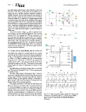
VI. SIMULATION AND MODELING OF SYSTEM (c)
The SIMULINK model of IH system with the PLL control (d)
circuit for the five levels inverter power supply is illustrated Fig. 4. PLL Base Control Simulation Model of IH System (a)
in Fig. 4 The parameters used in this model is R=26.6? , Overall IH Circuit Model (b) PLL Control Unit (c) PWM
L=120µH, C=0.08µF, sampling time 1µs , initial resonant Logic Circuit of Gate Signals (d) Variable Workpiece
frequency of the inverter fo=51.367 kHz, the applied DC Resistance
voltage source is 48 v. The value used for the Kc has been
calculated according to the “(8),”. The stability of the system
obtained when the value of integral gain Kc between 0 and
40×10-6.
The PWM signals introduced in Figure (4c) P1, P2, N1,N2
and PN0 has been illustrated in Fig. 5. The six gates signals
are shown in Fig.6:
The PLL output signal is illustrated in Fig. 7 which is
close to the sinusoidal waveform and this signal works as mod-
ulating signal in PWM. The phase angle difference between
inverter voltage vinv and capacitor voltage vc waveforms is
p/2 as shown in Fig. 8 and this difference changes after the
system detunes from resonant frequency.
The output waveform of XOR gate has 50% duty cycle
when the system in resonance state at resonant frequency
51.3 kHz as illustrated in Figure (9a) , but it will vary if the
system detunes from resonant state as illustrated in Figure
(9b) when the system operate at frequency 40kHz which is
below the resonant frequency. The duty cycle of XOR gate
will also detune if we choose frequency above the resonant.
As a result, the XOR output waveform in this PLL system