Page 119 - 2023-Vol19-Issue2
P. 119
115 |                                                             Al-Anbagi et al.

standardized to realizable values according to the market avail-
ability. The depicted values of the lumped elements in Fig-
ure 13 achieved the given gaols of S22 < -40 and S11 < -10
for the ±5 MHz around the operation frequency of 435 MHz.

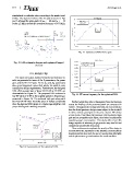
                                                                  Fig. 15. Optimized LNA’s Power gain

Fig. 13. LNA schematic diagram with optimized lumped
                             elements

                    III. RESULTS                                      Fig. 16. NF versus frequency for the optimized LNA

    The input and output-matched transistor performance re-           Further insight into other achievements from the literature
sults are presented in terms of the S-parameters, the power       versus the findings of the presented work are compared in
gain, and the NF. In Figure 14, the S11 and S22 parameters        Table II. Throughout this comparison table, we can clearly see
show good magnitude values that satisfy the satellite com-        how the listed previous designs were subject to the tradeoff
munications design requirements. Furthermore, the designed        to either achieve good gain at the price of poor NF values
LNA offers a power gain of about 26.149 dB at 435 MHz, as         or vice versa. Even when the previous LNAs achieved high
demonstrated in Figure 15. The proposed LNA achieved a            gain and an acceptable noise figure, they lacked consideration
low NF value of 0.459 at the targeted operation frequency,as      regarding power consumption. This study offered an LNA
presented in Figure 16. The achieved high gain along with         design capable of achieving high gain at a very low NF and
the very low NF were not at the price of design complexity        consuming considerably low power.
since the depicted LNA design is a single stage amplifier with
proper biasing and matching networks.                                 These achievements emphasis the novelty of this design to
                                                                  not only fulfill the aspirations of the satellite communications
                                                                  requirements but also meet the aim of constructing affordable
                                                                  and simple amateur ground stations for small satellites.

Fig. 14. S-parameters of the optimized LNA

