
Page 115 - 2023-Vol19-Issue2
P. 115
111 | Al-Anbagi et al.
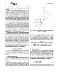
for satellite communications applications were reported in Fig. 1. The biasing network for the transistor (BFP840ESD)
[14–19] and should be examined in deep in the following to work as an amplifier
paragraph.
The collector current is (Ic= 2 mA), collector-emitter voltage
In [14], a 3-stage LNA was designed to serve GPS ap- (VCE=1 V), forward base-emitter voltage (VBE=0.8 V), and
plications at a frequency of 1.57 GHz, achieving a gain of DC current gain (hFE=250). Assuming the VCC voltage is
23.89 dB, a noise figure (NF) of 1.77 dB, and a power con- 1.2 V, the other elements of the biasing circuit are calculated
sumption of 6.54 mW. 2-stage LNA was reported in [15] for using the well-known biasing equations and listed in Table I.
satellite communications at 401.635 MHz resulting in a gain
of 28 dB and a relatively high NF of 3.6 dB. Another 2-stage TABLE I.
LNA for CubeSats at 29.15 GHz was presented in [16], where RESULTING BIASING CIRCUIT PARAMETERS
the achieved high gain was 39 dB but on the price of high-
power consumption of 420 mW and high NF of 2.8 dB. The Parameter IB RB1 RB2 Rc
study conducted in [17] was to design a LNA for CubeSats at
13-14 GHz consuming 162mW of power to generate a gain Value 8µA 10K? 4.54K? 96K?
of 15.5 dB and a NF of 2.4 dB. Serving the same previous
application and at the same operation frequency, the study
in [18] depicted an LNA design that consumes a higher power
of 3.2 W to produce a high gain of 54 dB while maintaining
almost the same NF of 2.3 dB. Lastly, the findings of LNA de-
signed for radar, nanosatellites, and GPS applications in [19]
revealed a wide-band operation frequency of 0.1-2 GHz with
a power gain of 11.3 dB and a high NF of 2.9 dB.
Enlightened by the surveyed LNAs in the literature, this
work presents an optimal LNA design for satellite communi-
cations ground terminals whose novelty is to achieve a high
gain of amplification and yet maintain very low NF. More-
over, the depicted LNA takes into consideration the power
consumption efficiency. As for this aimed LNA, the design
and simulation were conducted in the environment of AWR
Microwave Studio [20]. The rest of this article is organized
as follows: Section II describes the LNA design procedure,
including the biasing circuit, transistor stability verification,
and matching networks. Section III presents the study results
and compares findings versus previous designs. Section IV
briefly concludes the presented LNA achievements.
II. LNA DESIGN B. Transistor stability
The transistor can be either unconditionally stable or po-
After selecting (BFP840ESD) transistor for the intended
LNA design, the following parts describe in detail the de- tentially unstable based on the magnitude values of input and
sign procedure, including the biasing, stability, and matching output reflection coefficients, |Gin| and |Gout |. If |Gin| < 1and
networks. |Gout | < 1, the transistor is unconditionally stable. Otherwise,
the transistor’s stability may oscillate for different loads. The
A. Transistor biasing circuit unconditional stability factor (Rollet stability factor or K fac-
The biasing circuit of a transistor is necessary to ensure tor) is a measure of the LNA’s stability. It is calculated using
the transistor’s scattering parameters as in equation (1).
the operation in the active region. Figure 1 demonstrates the
biasing network for the transistor after connecting the biasing K = (1 - |S11|2 + |?S|2) (1)
elements. (|S12|2 - |S21|2)
For this NPN transistor to function as an amplifier, its where, S11 is the input reflection coefficient, S12 is the reverse
emitter-base and collector-base junctions must be forward transfer parameter, S21 is the forward transfer parameter, and
and reverse-biased, respectively. The datasheet of the selected
transistor (BFP840ESD) provides the following specifications: