
Page 118 - 2023-Vol19-Issue2
P. 118
114 | Al-Anbagi et al.
Fig. 11. Modified schematic of the matched stable transistor
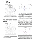
Fig. 9. NFCIR polar plot for evaluating input impedance The S11 and S22 curves in Figure 12 are not yet promis-
ing enough for the transistor to meet the requirements of the
the required lumped elements at the input matching network. LNAs for small satellites. Figure 12 shows an input reflection
Similarly, from S22 polar plot, we get the output impedance coefficient of -0.32 dB which emphasis the almost total reflec-
of 1.251 - 0.161i, which becomes 62.55 - 8.05i after normal- tion of the input power at the input port. On the other hand,
ized to 50 ?. The schematic diagram in Figure 11 shows the resulting reflection coefficient at the output port indicated
the input and output matched transistor with the calculated the perfect matching of that port to the terminated load.
lumped elements.
Thus, the lumped elements were optimized using the AWR
optimizer algorithm of Particle Swarm. Particle Swarm is a
well-known optimization algorithm that can be used to find
optimal values of several variables after setting certain goals
to meet. This algorithm is a built-in option in AWR and was
used to evaluate the optimal values of the lumped elements
to achieve the requires S11 and S22 goals of (< -10) and
(< -40), respectively. These introduced goals must be met
within the frequency range of (430-440) MHz which repre-
sents a ±5 MHz around the operation frequency of 435 MHz.
Fig. 10. S22 polar plot for evaluating output impedance
The performance of the transistor after the matching net- Fig. 12. S-parameters after terminating matching networks
works design is again observed through the S11 and S22 pa-
rameters and presented in Figure 12. The optimized lumped elements are terminated to the tran-
sistor as in Figure 13. The optimized lumped elements were