
Page 186 - 2023-Vol19-Issue2
P. 186
182 | Gaid & Ali
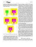
antenna and specifying its properties, such as thickness, di- the inset feed technique as seen in Fig. 1 (b). The updated
electric constant, and loss tangent, is important. Fig. 1 illus- design achieved resonance at 28 GHz and a return loss of
trates the five major phases involved in developing the final approximately 36 dB, while a new frequency band around
optimized antenna design. 46 GHz was observed. In the third phase, an I-shaped slot
was etched horizontally on the upper side of the patch as
seen in Fig. 1 (c), which slightly improved the return loss
at around 42 GHz, while the resonance remained at 28 GHz
with a slight decrease in the return loss value. In the fourth
phase, a second I-shaped slot was etched perpendicular to the
previous slot on the left side of the radiating patch as shown
in Fig. 1 (d). The resonance in the second band shifted to the
left, with a noticeable improvement in the value of its return
loss. A third band around 63 GHz also appeared with the
inclusion of the second slot. To cover the frequency ranges
of 28 GHz, 38 GHz, and 60 GHz, a third I-shaped slot was
etched perpendicular to the first horizontal slot, forming the
symbol p as seen in Fig. 1 (e). After adding the third slot, the
resonant frequency in the second band moved to around 38
GHz, while the resonant frequency in the third band moved to
around 56 GHz, with a clear improvement in the return loss
values in the second and third bands. It is observable that the
insertion of slots on the radiating element causes only a very
slight shift in resonance at 28 GHz. This unnoticeable shift
could be because slots’ insertions did not significantly alter
the current distribution at that resonance frequency. However,
the return loss value is affected by the insertion of slots.
Fig. 1. The development of the proposed tri-band antenna. B. The Final Optimized Design
Figure 2 depicts the final optimized tri-band antenna geometry,
Initially, the antenna design utilized the dielectric material which consists of a rectangular patch on the top face of the di-
RT/Duroid 5880, which has a dielectric constant of 2.2 and a electric substrate material and a copper sheet with a thickness
loss tangent of 0.0009, and targeted a frequency of 28 GHz. of 0.035 mm on the opposite face. The substrate material’s
However, the initial design, shown in Fig. 1 (a) exhibited size is 8 × 8.5 × 0.508 mm³, and the patch has a p-shaped slot
poor return loss performance and resonated at 53 GHz. To and is fed by a microstrip line connected through an inset feed.
enhance the return loss performance, the matching between The optimal dimensions of the final design are summarized in
the radiating patch and its feeding line was improved using Table I.
The S11 performance of the antenna throughout the five
phases of the design process is shown in Fig. 3. The blue
dashed line represents the S11 performance of the final opti-
mized design, which has resonance frequencies of 27.9 GHz,
38.4 GHz, and 56 GHz, operating in three bands: 28 GHz,
38 GHz, and 60 GHz. The relative return loss levels for each
band are 15.4 dB, 18 dB, and 26.4 dB, respectively. The band-
widths for each band are adequate, with the first spanning
from 27.245 to 28.505 GHz, the second spanning from 37.775
to 38.855 GHz, and the third spanning from 51.725 to 63.74
GHz.
III. PARAMETRIC ANALYSIS
To achieve the necessary frequency bands with a wide fre-
quency range and improve impedance matching, a parametric