
Page 107 - 2023-Vol19-Issue2
P. 107
103 | Abdulzahra, Alnahwi & Abdullah
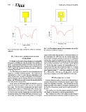
Fig. 2. (a) The basic shape and (b) the reflection coefficient Fig. 3. (a) The radiator element with rectangular slot and (b)
response. the reflection coefficient response.
III. PIN DIODE CONFIGURATION AND square annular patch that operates as a wideband antenna.On
the other hand, the OFF-state cuts the antenna patch into
OPERATION two unequal monopole antennas to operate as a dual-band
antenna.Fig. 6 depicts the equivalent circuits of a PIN diode
PIN diodes can be used to design frequency reconfigurable at its ON and OFF states [7].It is merely an RL series circuit
antennas by controlling the effective length of the radiating el- with an inductor labeled ”L” and a low-value resistor labeled
ement. By incorporating multiple PIN diodes into the antenna ”R1” for the ON-state. However, it is comparable to an RLC
design, different parts of the antenna can be switched ON or circuit in the OFF-state with an inductor named ”L” in series
OFF to switch the antenna frequency response to different with parallel combination of a high-value resistor named ”R2”
operating frequencies. and a capacitor named ”C”. It has been modeled in CST with
R1 = 0.85 ?, R2 = 0.85 ?, L = 0.7 nH, and C = 0.21 pF,
The PIN diode can be modeled in a reconfigurable antenna according to datasheet of the SMP1340-079LF PIN diode.
design as a variable reactance element. The model can be
represented as a shunt or series element, depending on the IV. PARAMETRIC STUDY
design requirements. In a shunt configuration, the PIN diode is
placed in parallel with the radiating element. In the proposed Antenna dimensions play a critical role in determining its
design, one PIN diode was used to ensure the reconfigurability operating characteristics, including its radiation pattern, band-
from wide band to bi-band [22]. width, and impedance matching. These dimensions are the
length and width of the radiator, the length of partial ground,
In this work, one PIN diode (SMP1340-079LF) is used to the feed line dimensions, as well as the length and width of
switch the frequency response of the antenna from wideband the slits.
to bi-band. The PIN diode exhibits open and short circuit
behavior that results in a reorganization of the antenna oper- The insertion of a slit in the antenna radiator has a signifi-
ating frequency and a change in its effective resonant length. cant impact on the antenna’s operating characteristics.
In order to ensure that the appropriate current density flows
through the radiator, the ON and OFF states of diodes are used. Fig. 7 displays the effect of slit width g and slit length d
As a result, the ON-state of the diode results in a complete on the ON-state antenna reflection coefficient response. The