
Page 106 - 2023-Vol19-Issue2
P. 106
102 | Abdulzahra, Alnahwi & Abdullah
conclusion.
II. ANTENNA DESIGN
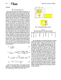
The structure of the proposed antenna is shown in Fig. 1. A Fig. 1. The proposed antenna structure.
monopole patch antenna is used to obtain a wide bandwidth,
which is characterized by its partial ground plane. The struc- TABLE I.
ture of the monopole patch antenna typically consists of the The initial dimensions of the proposed antenna
following main components: radiating element, ground plane,
dielectric substrate, and feed line. The radiating element is Parameter Dimension (mm) Parameter Dimension (mm)
a metal patch that is located on the top layer of a dielectric 19 Lp 9
substrate. In the top layer of the substrate, the rectangular Ws 26 Lf 12
metal patch of the proposed antenna is fed by a microstrip Ls 9.5 Wf 3
line. The ground plane of a monopole patch antenna is a Lg 11
conductive layer that is located on the bottom layer of the Wp
dielectric substrate. The ground plane serves as a reflecting
surface for electromagnetic energy radiated by the patch. The The microstrip antenna is transformed into a planar monopole
dielectric substrate is a non-conductive material that separates antenna by the partial coverage of the ground plane to convert
the radiating element and the ground plane. The feed line is a it from ?g/2 resonator to ?g/4 resonator [21]. In Fig. 3(a),
transmission line that connects the monopole patch antenna the parameter values are modified by engraving 4×4.5 mm2
to the transmitter or receiver. The initial structure is based on rectangular slot on the radiating patch. The reflection coef-
the basic shape of the rectangular monopole antenna shown ficient also has wideband coverage with -10 dB bandwidth
in Fig. 2(a) using the low-cost FR4 substrate, which has a covering the range (3-9) GHz as shown in Fig. 3(b). After
dielectric constant of 4.3, a loss tangent of 0.025, and a height that, a slit of 1 mm width is inserted to make two unequal
of 1.6mm. The microstrip feed line characteristic impedance monopole antennas as shown in Fig. 4(a). As can be seen in
is set to be 50 ?. The overall dimensions of the proposed an- Fig. 4(b), this step leads to a dual-band centered at 3 GHz and
tenna are 26mm × 19mm, and the initial parameters are given 6.4 GHz with -32.35 dB and -22.75 dB, respectively. Finally,
in Table I. The reflection coefficient of the initial design is another slit is engraved on the shorter monopole as illustrated
shown in Fig. 2(b), whose -10dB bandwidth covers the range in Fig. 5(a) to increase the length of the current path of the
(2.98-8.37) GHz. The conventional design equations for the antenna that leads to shifting the resonant frequency down to
initial monopole antenna at a center frequency of fo=3.5 GHz 3 GHz and 6 GHz as shown in Fig. 5(b). The PIN diode used
are as follows [21]: to switch the operation of the antenna is SMP1340-079LF.
The purpose of inserting the PIN diode is to accomplish the
W= c (1) frequency reconfigurability as will be explained in the next
section. The ON-state of the PIN diode results in a complete
2 fo er +1 square ring with wideband operation, while the OFF-state
2 results in a dual-band operation due to the presence of the two
unequal monopoles.
L= c - 0.824h[ (ere f f + 0.3)( W + 0.264) ] (2)
v (ere f f - h + 0.8)
fo ere W
2 f f 0.258)( h
Zo = 120p (3)
v f [ Wf + 1.393 + 0.667ln( Wf + 1.444)]
ere f h h
ere f = er + 1 + er -1 h -1 (4)
2 [1 + 12
f ]2
2 Wf
where W is the patch width, fo is the antenna resonant
frequency, L is the radiator length, er is the substrate dielectric
constant, ere f f is the substrate effective dielectric constant, h
is the substrate height, and Wf is the feedline width.