Page 293 - 2024-Vol20-Issue2
P. 293

289 |                                                                                                                    Abdulabbas & Salih

                                                                               Vcarrie                     vb* vc*
                                                                   Vp
                                                                                                                                                t
                                                                                          r

                                                                                       va*
                                                                   -Vn

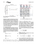
Fig. 6. Changing of duty cycle with constant outer                 S1
parameters in qZSI.                                                                                                                                                             t

this approach, the duration of shoot-through time remains con-     S2
sistent for each switching cycle, ensuring a steady boost factor.                                                                                                               t
The shoot-through duty ratio drops as the modulation index
M increases in this manner. Therefore, the highest possible        S3
shoot-through duty ratio is restricted to (1 - M). When the                                                                                                                     t
value of M grows to its maximum, the shoot-through duty
ratio reaches zero, causing the inverter to operate in the same    S4
way as the typical VSI. The direct current (DC) inductor cur-                                                                                                                   t
rent and capacitor voltage do not exhibit any fluctuations that
are linked to the output frequency.                                S5
                                                                                                                                                                                t

                                                                   S6
                                                                                                                                                                                t

                                                                                                 Shoot
                                                                                                through
                                                                                                 region

                                                                      Fig. 7. Simple boost modulation of qZSI circuit.

                                                                   Vg = vga vgb vgc T, Li = Lia Lib Lic ,
                                                                   Lo = Loa Lob Loc , and C = Ca Cb Cc respectively.

                                                                   The three-phase grid voltage are given by vga = Vg cos(?t) ,
                                                                                                   2p                                  2p
                                                                   vgb = Vg cos    ?t           -  3   , andvgc = Vg cos      ?  t  +  3     since the

                                                                   current injected into the grid is required to be sinusoidal

                                                                   and in phase with the grid voltage so the reference grid

                                                                   current should be selected as following ioa* = I*o cos(?t) ,
                                                                   iob* = I*o cos                  2p  , and ioc* = I*o cos            2p
4) Three-phase grid-tied VSI                                                       ?         t  -  3                          ?t  +    3     .
Fig. 1 clearly shows that the dc-link voltage of the VSI corre-
sponds to the output voltage of the qZS network. The Voltage       The  pole  voltages          can    be  obtained  as  VIN  =     1  (1 +  sk)Vdc                                as
Source Inverter (VSI) is linked to the electrical grid through a                                                                    2
Low Pass Filter (LCL). By utilising Kirchhoff’s voltage and
current rules to analyse the circuit depicted on the right of the  k=a,b,c and sk is switching function given by the following
qZS network, one can derive the subsequent set of differential
equations.                                                         equation

                                                                        sk =       +1 if si is closed
                                                                                   -1 if si is closed

L1  di1  +  r1i1  =   Vinv  - VC                    (8)            Since Vinv = ViN - VnN
    dt                                                             So, The phase to neutral voltage expressions in terms of input

                                                                   voltage and switching function

Lo  dio  +  roio  =   VC  -  Vg                     (9)                 Vinv =           ?              2  -1  -1 ? ? sa ?                      (11)
    dt                                                                             1                   -1   2  -1 ? ? sb ?
                                                                                   6 Vdc ?             -1  -1   2 sc

C dVC    =  ii  - io                                (10)           It can be transformed the three-phase quantity to the syn-
   dt                                                              chronous reference dq frame oriented by d-axis and neglected

Where the matrices are given by ii = iia iib iic T ,Vinv =         zero sequence component so the all AC quantities become DC
                                                                   hence this purpose using Park transformation to obtain differ-
van vbn vcn T , VC = vca vcb vcc T, io = ioa iob ioc Te, nt variables of this circuit. Applying this transformation can
   288   289   290   291   292   293   294   295   296   297   298