Page 117 - 2024-Vol20-Issue2
P. 117
113 |                                        Maddu & Bhasme

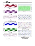
       (a) Phase Voltage                     (a) Reference and Carrier Signal generation for SPWM
       (b) Line Voltage

                          (c) Load Current            (b) Phase Currents in SPWM

Fig. 10. SVPWM (Min-Max) simulation results  (c) Reference signal in SVPWM (Min-Max)

                          (a) Phase Voltage   (d) Phase currents in SVPWM (Min-Max)

                           (b) Line Voltage       Fig. 12. Hardware results

                          (c) Load Current

       Fig. 11. THPWM simulation results

