Page 110 - 2024-Vol20-Issue2
P. 110
106 |                                                                                                         Maddu & Bhasme

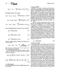
vleg,c       =  Vdc  ·  dc  =  Vdc   M  Sin(2p   f  t  +  2p  /3)      +     Vdc   (7)  1) Sinusoidal PWM
                                2                                             2         In SPWM, the three-phase modulating sinusoidal signal is
                                                                                        compared to a high-frequency carrier signal to generate gate
The fundamental line-to-line voltages                                                   pulses at a fundamental frequency (50 Hz) for the inverter
                                                                                        switches. Assume that the reference sine wave (Rotor output
                                      v 3Vdc                                            desired waveform) is compared to the carrier signal (Ramp
                                        2                                               ranges from 0 to 1). If the reference signal is a higher ampli-
?vab? = vleg ,a - vleg, ,b =                  M  cos(2p       f  t  -     p  /3)   (8)  tude than the carrier signal amplitude then the switch is in an
                                                                                        ON state (1) and if the reference signal is less than the carrier
                                         v3Vdc                                          signal then the switch is in an OFF state (0). The amplitude
                                          2                                             modulation index is defined as “The peak value ratio of the
?vbc? = vleg,b - vleg,c =                        M     cos(2p       f  t  -  p  )  (9)  sinusoidal modulating signal to the carrier wave peak” i.e.,
                                                                                        Ka = V m/V c
                                     v  3Vdc
                                        2                                                   There are two regions named linear region of modula-
?vca? = vleg,c - vleg,a =                     M  cos(2p   f   t  +     p  /3)     (10)  tion and Over modulation that SPWM can operate. For the
                                                                                        Linear region of modulation 0 < Ka = 1, the inverter output
Hence, the fundamental phase voltages (i.e., line-to-neutral):                          voltage (phase or line) increases linearly with the Amplitude
                                                                                        modulation index, Ka. For the Over-modulation Ka > 1, the
?va?      =   Vdc  M  sin(2p   f  t)                                              (11)  inverter output voltage (phase or line) increases non-linearly
               2                                                                        with the Amplitude Modulation index, Ka. To implement
                                                                                        the SPWM technique for Motor control applications, a high
?vb?      =   Vdc  M  sin(2p   f  t  -  2p /3)                                    (12)  carrier frequency signal (Generally 10 kHz to 20 kHz) is gener-
               2                                                                        ated from a microcontroller which is compared to a reference
                                                                                        modulating signal (Generated from a controller). To avoid
?vc?      =  Vdc   M  sin(2p   f  t  +  2p /3)                                    (13)  the harmonics mixed up with the fundamental frequency, the
              2                                                                         frequency of the carrier or ramp is at least 10 times greater
                                                                                        than the fundamental frequency [8, 18]. The phase to neutral
                                                                                        voltage can be written as,

Using the equations of phase voltages, load or phase can be                             van = 0.5Vdc sin(wt)  (17)

written as follows                                  MiVdc                         (14)  2) Space vector PWM
                                        v        R2 + (2p f L)2                         In a three-phase inverter, the switches can turn on and off
                                           2                                            in eight unique states. By joining the sides of the vectors
                                                                                        and making them into a hexagon. The main objective is to
       Ia,RMS = Ib,RMS = Ic,RMS = 4                                                     find the maximum phase to neutral voltage and generate the
                                                                                        different switching patterns in a different way than the SPWM
Where Mi refers modulation index, R and L represent resis-                              technique. Strictly speaking, it will look Cube in a three-
tance and Inductance respectively.                                                      dimensional view, the same seems to be a hexagon in two- a
                                                                                        dimensional view. It is impossible to produce a voltage vector
    In a Six-Step/ Square Wave Inverter, the phase-to-neutral                           that is beyond this hexagon as a modulation would exceed a
voltage and the line-to-line voltage (in terms of the Fourier                           hundred percent which cannot happen. For Sine Wave gen-
Series) can be written as                                                               eration, a voltage vector of constant magnitude is needed in
                                                                                        every direction. The magnitude of the voltage vector is equal
             2 11                                                                       to the phase to neutral voltage. This voltage vector is obtained
van(t) = Vdc         sin wt + sin 5wt + sin 7wt + . . . .                         (15)  using the Clarke transform. The magnitude of the voltage
           p                   57                                                       vector doesn’t change in the case of Clarke Transformation.
                                                                                        By using Space Vector Modulation, there is 15% more voltage
          v                                 1                                           can be produced as compared to the SPWM technique [4].
          23                             + sin 5                                        In conventional SVPWM, the basic idea is to attain the de-
vab(t) =      Vdc    sin    wt - p                     wt - p             +...          sired voltage vector by taking the average of different possible
          p                       6         56                                 (16)     states. However, the switching states are moving from one

B. PWM techniques
In the following subsections, different PWM techniques have
been discussed.

